Photoresist Track Technology: The Quiet Enabler Behind Specialty Chips and AI Infrastructure
October 22, 2026 - 09:02
Semiconductor investment tends to focus on the most visible parts of the manufacturing chain, especially lithography exposure tools. But patterning depends on more than exposure. Photoresist coating and developing tracks apply resist, manage thermal cycles and develop patterns that later steps rely on. Track performance shapes coating uniformity, defect levels, throughput and overall manufacturing economics. That matters in high-volume 300mm silicon fabs, and it matters just as much in compound semiconductors, photonics, MEMS, power devices and advanced packaging, where substrates, resist thicknesses, wafer sizes and production volumes often differ from mainstream logic and memory work.
These specialty segments are gaining importance as AI infrastructure raises demand for optical communications, power management and heterogeneous packaging. That opens room for equipment designs that prioritize wafer-handling efficiency, processing flexibility, compact footprints and cost of ownership.
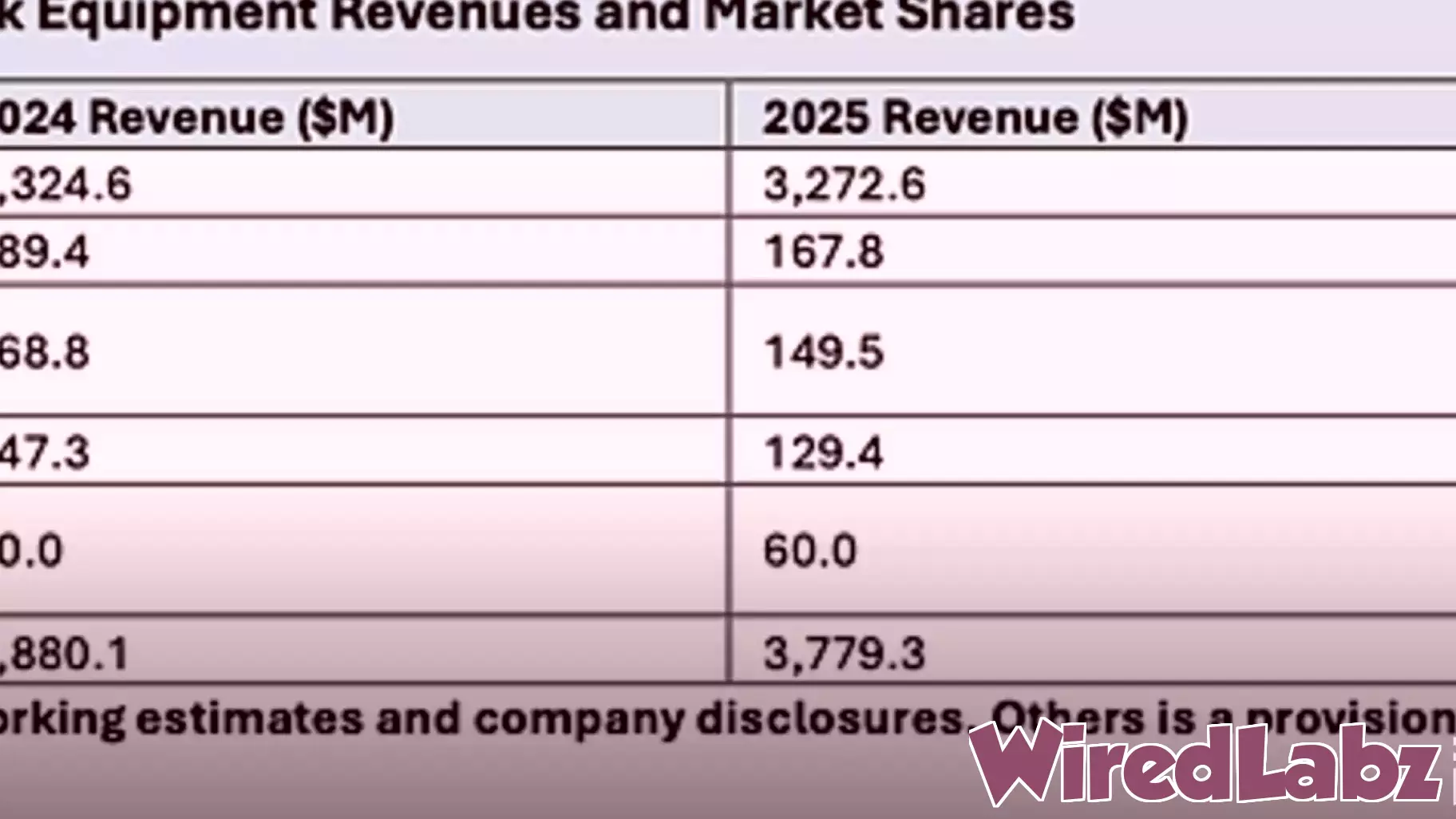
The global photoresist track equipment market is estimated at about 3.78 billion dollars in 2025, down 2.6 percent from 3.88 billion dollars in 2024. Tokyo Electron holds an estimated 86.6 percent share, followed by SEMES at 4.4 percent, SCREEN at 4.0 percent and Kingsemi at 3.4 percent. That concentration reflects the importance of established platforms in high-volume manufacturing, but overall share does not capture conditions in specialty fabs, where substrate flexibility, small-lot efficiency and capital cost often carry more weight.
300mm systems account for roughly 3.33 billion dollars, or 88.1 percent, of 2025 track revenues. Equipment for 200mm and smaller wafers accounts for about 449.3 million dollars, or 11.9 percent. By application, silicon front-end manufacturing represents approximately 3.40 billion dollars, or 89.8 percent. Advanced packaging contributes 243.8 million dollars, or 6.5 percent, and specialty applications including compound semiconductors, MEMS, photonics and power devices add 140.5 million dollars, or 3.7 percent. Advanced packaging and specialty applications together represent about 384.3 million dollars, and both connect directly to the buildout of AI infrastructure.
Track architecture can strongly influence manufacturing economics. Conventional systems combine coating, developing, thermal processing, chemical delivery and wafer handling into coordinated platforms. As module counts rise, wafer transport can become a bottleneck if the handling system cannot supply and remove wafers fast enough to keep process stations busy. Two useful indicators when evaluating handling are the number of end effectors and the number of controlled motion axes. More end effectors can increase the number of wafers ready for exchange. Fewer axes can reduce actuators, drives, sensors and mechanical complexity. Footprint also matters, since cleanroom expansion often requires major investment in environmental controls, chemical distribution and exhaust infrastructure.
S-Cubed, a New Jersey equipment maker with decades of photoresist processing experience, developed its Quad Z Trac as an alternative to conventional central-robot architecture. The core is a three-axis process robot with four end effectors, supported by a five-axis front-end robot with two end effectors. Instead of relying mainly on extra robot movements to service modules, Quad Z stages multiple wafers for exchange. S-Cubed describes the result as a move-swap approach rather than a swap-move-swap sequence. Removing a completed wafer while a replacement is already available is intended to cut unproductive transfer motion and raise process-module utilization.
S-Cubed reports that Quad Z can accommodate roughly twice as many process modules within a footprint comparable to certain conventional central-robot configurations. Its compact 200mm implementation is specified at less than 25 square feet, including the chemical cabinet. The company's FLEXI development platform shares related processing approaches with Quad Z, creating a potential path from development recipes to production equipment.
For specialty manufacturing, cost per good wafer is a more useful measure than headline throughput. Capital cost, utilization, floor space, maintenance, process flexibility, yield and qualification burden all feed into that number. Quad Z addresses these factors through four design choices: four process-robot end effectors to reduce idle transfer movements, a three-axis process robot to limit mechanical complexity, a modular architecture for high process-station density in a compact footprint, and support for varied substrates and processes. The potential advantage is cumulative, since better scheduling can improve utilization while compact equipment and simpler mechanics can lower facility and maintenance burdens. Real advantages in cost per good wafer will still need to be shown through customer data covering throughput, yield, defectivity, uptime and maintenance.
The immediate opportunity for S-Cubed lies in applications where conventional high-volume silicon equipment may not fit customer needs. Compound semiconductor, photonics, MEMS, power device and advanced packaging manufacturers often require flexible resist processing, support for nonstandard substrates and efficient handling of small lots. Quad Z is designed for multiple wafer materials and diameters, including silicon, GaAs, InP,
MORE NEWS

October 21, 2026 - 17:32
A New Security Flaw Is Pushing Websites OfflineA wave of website shutdowns is spreading across the internet as operators scramble to defend against a newly discovered security vulnerability. The flaw, which appears to allow automated tools to...

October 21, 2026 - 04:37
AI leading to more work, not less, according to new studySAN FRANCISCO (KRON) - One of the most common claims about AI is that the technology will somehow give us more of our time back by automating the more repetitive, mundane tasks we perform at work....

October 20, 2026 - 07:12
Apple Hit With Lawsuit Over Face Recognition TechA new lawsuit filed against Apple claims the company`s facial recognition technology violates user privacy rights. The legal action centers on how Face ID collects and stores biometric data,...

October 19, 2026 - 21:55
Broadcom and Micron Take Different Paths in the AI Chip RaceThe AI hardware boom has lifted demand across the semiconductor industry, but two companies stand out for very different reasons. Broadcom supplies custom accelerators and networking silicon that...