Anticipating the Hardware Innovations of 2027
11 September 2026
Hardware roadmaps move slowly in public and quickly in private. The products that will define 2027 are already silicon in a lab, a reference design on an engineer's bench, or a specification locked inside a standards body. What follows is not a prediction of specific product names. It is an analysis of the physical and economic forces that will shape what ships, why certain approaches will win, and where the genuine trade-offs will land for buyers, builders, and IT decision makers.
The central theme is constraint. For two decades, hardware improved because transistors got smaller and cheaper on a predictable cadence. That cadence has slowed at the leading edge, while demand for compute has accelerated. The innovations arriving around 2027 are largely responses to that gap. They are less about raw scaling and more about packaging, specialization, power delivery, memory architecture, and manufacturing economics.
The End of Easy Scaling and What Replaces It
Moore's Law was never a law. It was an observation about economic incentive: shrinking transistors made them faster, cheaper, and more power efficient at the same time. Around the mid 2010s, that triple benefit broke apart. Smaller nodes still improved density and efficiency, but cost per transistor stopped falling at the same rate. Design costs for a leading edge chip now run into the hundreds of millions of dollars, and only a handful of companies can justify them.The industry response has been to stop treating a chip as one monolithic piece of silicon. Instead, it splits functions across multiple smaller dies, manufactured on different nodes, and joins them in a single package. This is chiplet based design, and by 2027 it will be the default for anything above mid range.
Why it works: a small die has a higher yield than a large one because defects scale with area. If you build a 600 square millimeter monster and one defect lands on it, you scrap the whole thing. If you build six 100 square millimeter dies and one is defective, you lose one sixth of the output. The economics favor disaggregation even before you account for the ability to put cache on a cheap mature node and logic on an expensive leading node.
The trade-off is real and often understated. Chiplets introduce new failure modes. The interconnect between dies costs power and adds latency. Thermal density becomes harder to manage because heat is now concentrated in small hotspots rather than spread across a large die. Testing gets more complex, and a package level defect can waste several good dies at once. Companies that rushed into chiplets without solving these problems have shipped products with uneven performance across units, which is a nightmare for anyone trying to guarantee consistent behavior in a data center.
For buyers, the practical implication is that benchmark numbers will matter less than consistency. Two chips with the same model number may perform differently depending on how many chiplets passed validation. Ask vendors about performance variance, not just peak throughput.

Advanced Packaging Becomes the Real Battleground
If chiplets are the strategy, advanced packaging is the tactic that makes it possible. Packaging used to be an afterthought, a plastic or ceramic shell that protected the die and routed signals to the board. It is now a performance critical technology.Three approaches matter for 2027.
The first is 2.5D packaging, where multiple dies sit side by side on a silicon interposer that provides dense wiring between them. This is how high bandwidth memory has been attached to GPUs and accelerators for years. The interposer is expensive and limited in size, but it delivers enormous bandwidth per watt compared to routing signals across a printed circuit board.
The second is 3D stacking, where dies are placed directly on top of each other and connected with vertical vias. This dramatically shortens interconnect distance, which cuts latency and power. The hard part is heat. If you stack a power hungry logic die under a memory die, the memory cooks. Solutions involve putting the hottest layer on top, using thinner dies, and adding thermal pathways, but the physics impose a ceiling on how much power you can push through a stack.
The third is hybrid bonding, which joins dies with copper to copper connections at a pitch measured in single digit microns. Compared to solder bumps, hybrid bonding allows far more connections per unit area and lower electrical resistance. It has been used in image sensors for years and is now moving into logic and memory. By 2027, expect hybrid bonding to be a standard option for high end mobile processors and accelerators, though cost will keep it out of budget parts.
The practical question for anyone specifying hardware is whether the packaging technology actually helps their workload. A workload that is memory bandwidth bound will benefit enormously from 2.5D integration with high bandwidth memory. A workload that is compute bound and cache friendly may see little gain. Packaging is not a universal upgrade. It is a targeted fix for specific bottlenecks.
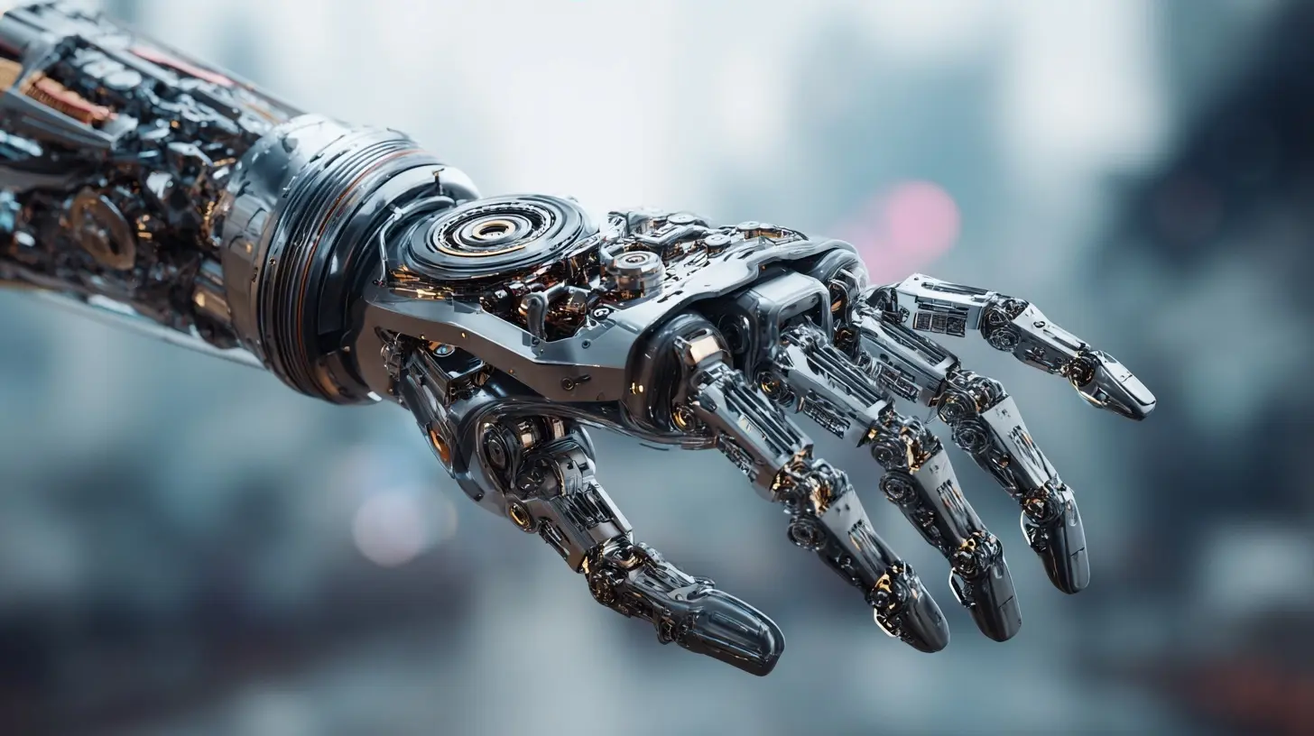
Memory and Storage: The Quiet Revolution
Memory is where the most consequential changes will happen, partly because it has been the biggest bottleneck in real systems for years. Processors got faster. Memory latency barely moved.HBM, or high bandwidth memory, stacks DRAM dies vertically and connects them through a wide interface. The latest generations deliver bandwidth measured in terabytes per second per package. The problem is cost and capacity. HBM is expensive to manufacture and hard to scale beyond a certain stack height. By 2027, expect HBM to remain the choice for accelerators and top tier server CPUs, while mainstream systems use more conventional DDR variants.
The more interesting development is the push to put memory closer to compute in ways that change the programming model. Compute express link, or CXL, allows memory to be pooled and shared across processors over a high speed link. This matters because most servers waste memory. A machine running a database might use 60 percent of its RAM while the machine next to it is starved. CXL lets operators pool memory and allocate it dynamically.
The catch is latency. CXL attached memory is slower than local DRAM, so it works well for capacity expansion and less well for latency sensitive workloads. Expect 2027 to bring clearer guidance from vendors about which workloads benefit. The honest answer is that CXL is transformative for some use cases and irrelevant for others. Anyone who tells you it is a universal win is selling something.
On the storage side, the shift is from interfaces to media. PCIe generations keep doubling bandwidth, and by 2027 PCIe 6.0 will be shipping in volume. But the real change is the maturation of storage class memory and the increasing intelligence inside SSDs. Modern drives have their own processors and can perform compression, encryption, and even rudimentary database operations internally. This offloads work from the host CPU, which matters as CPU cores become more specialized and less general purpose.
The risk is complexity. An SSD that does too much becomes a black box that is hard to debug and hard to tune. Best practice for 2027 will be to use drives that expose their internal behavior through standard telemetry, and to avoid vendor specific features that lock you in.
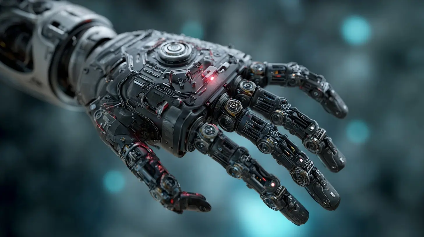
Power Delivery and Thermal Management
Every generation of hardware pushes more power through the same physical space. A rack that drew 10 kilowatts a decade ago may draw 40 or more today. This is not a peripheral concern. It is the constraint that shapes everything else.Voltage regulator modules, or VRMs, convert the power supply's voltage to what the chip needs. As currents rise, resistive losses in the VRM and the board become significant. The industry is moving toward vertical power delivery, where the VRM sits directly under the processor rather than beside it. This shortens the path and reduces losses. By 2027, expect vertical power delivery to be common in high end servers and increasingly in premium laptops.
Cooling is following a similar trajectory. Air cooling has limits, and those limits are being hit in dense racks. Liquid cooling, once exotic, is becoming standard in data centers that run accelerators. The options range from direct to chip cold plates, where liquid flows through a metal block attached to the processor, to immersion cooling, where entire servers are submerged in a non conductive fluid. Direct to chip is easier to retrofit and easier to service. Immersion is more efficient but requires new operational practices and makes maintenance harder.
The trade-off is operational, not just technical. Liquid cooling introduces leak risk, requires new skills for data center staff, and complicates the supply chain. For organizations that run modest density, air cooling will remain viable and cheaper. For anyone running dense accelerator clusters, liquid is no longer optional.
The Rise of Domain Specific Silicon
General purpose CPUs are not going away, but they are no longer where the performance gains are. The gains are in specialized silicon: accelerators for machine learning, video encoding, cryptography, networking, and storage.The reason is straightforward. A general purpose core spends most of its transistors on flexibility, branch prediction, out of order execution, and caches that may or may not be useful for a given workload. A specialized unit strips that away and spends its area on the operations that matter. The result is often an order of magnitude improvement in performance per watt for the targeted task.
The problem is that specialization is a bet. If the workload changes, the silicon becomes dead weight. This is why the industry has converged on a middle path: reconfigurable logic and domain specific architectures that can be reprogrammed for related tasks. Field programmable gate arrays sit at one end of that spectrum. At the other end are accelerators with enough programmability to handle a family of related workloads rather than a single fixed function.
For decision makers, the guidance is to match the degree of specialization to the stability of the workload. If you know the workload will not change for five years, a fixed function accelerator is the most efficient choice. If the workload is evolving, a more programmable option costs more per operation but protects you from obsolescence. The most common mistake is buying specialized hardware for a workload that is still in flux, then discovering the hardware cannot adapt.
What This Means for Different Buyers
The innovations of 2027 will land differently depending on who you are.For consumers, the most visible change will be in mobile devices. Expect better battery life rather than dramatically faster phones, because the gains are going into efficiency and into on device machine learning. The practical advice is to stop chasing peak benchmark scores and start looking at sustained performance and thermal behavior. A phone that is fast for thirty seconds and then throttles is worse than one that is moderately fast indefinitely.
For laptop buyers, the divide between ARM based and x86 based machines will widen. ARM designs have an efficiency advantage that matters enormously in thin and light devices. x86 retains an advantage in legacy software compatibility and in raw single threaded performance for certain tasks. By 2027, the choice will be less about brand and more about which ecosystem your software runs best on. Test your actual workload before committing.
For data center operators, the decisions are harder. The move to liquid cooling, the adoption of CXL memory pooling, and the shift to chiplets all require capital investment and operational change. The right sequence is to pilot one change at a time, measure the actual benefit, and only then scale. Organizations that try to adopt everything at once tend to fail, because the interactions between new technologies are hard to predict.
For hardware startups and system builders, the barrier to entry is rising. Designing a chip now requires access to advanced packaging, which is concentrated in a few facilities, and to leading edge foundry capacity, which is expensive and allocated years in advance. The opportunity is in the layers around the chip: cooling, power delivery, interconnect, and software that makes specialized hardware usable. Those are less capital intensive and increasingly where the value accrues.
Common Misconceptions Worth Correcting
A few beliefs are widespread and wrong.The first is that smaller process nodes always mean better performance. They mean better density and usually better efficiency, but a chip on a mature node with a good architecture can beat a poorly designed chip on a leading node. Architecture matters more than node for most workloads.
The second is that more cores always help. They help when the workload parallelizes well. For many tasks, a few fast cores beat many slow ones. This is why high end desktop and server chips still prioritize single threaded performance alongside core count.
The third is that new memory technologies will replace existing ones quickly. They rarely do. DDR4 is still in wide use years after DDR5 launched, because the cost per gigabyte and the ecosystem of compatible hardware take time to shift. Expect the same gradual transition for CXL and for storage class memory.
The fourth is that power efficiency and performance are opposites. At the system level, they often align. A more efficient chip runs cooler, which lets it sustain higher clocks for longer. Efficiency is not a compromise. It is often the path to sustained performance.
Practical Recommendations
If you are planning hardware purchases or infrastructure for 2027, a few principles will serve you well.Buy for sustained performance, not peak. Ask vendors for thermal design power, throttling behavior, and real world benchmarks that run for at least thirty minutes. Peak numbers are marketing.
Prioritize memory bandwidth and capacity over raw compute if your workloads are data heavy. Most modern bottlenecks are in the memory subsystem, not the arithmetic units.
Treat cooling and power as first class design constraints. If you are planning a dense deployment, budget for liquid cooling and for the operational changes it requires. Retrofitting later is expensive and disruptive.
Demand telemetry from your hardware. As systems become more complex, the ability to see what is happening inside them becomes essential. Avoid components that are opaque.
Pilot before you scale. New technologies rarely behave as advertised in production. A small deployment that surfaces problems early is worth more than a large one that fails publicly.
Plan for heterogeneity. The era of one architecture fitting all workloads is ending. Your infrastructure will increasingly mix general purpose and specialized components, and your software stack needs to handle that.
The Bottom Line
The hardware innovations arriving around 2027 are not about a single breakthrough. They are about a collection of engineering responses to a world where scaling is harder and demand is higher. Chiplets, advanced packaging, new memory architectures, liquid cooling, and domain specific silicon are all attempts to extract more capability from physical limits that are no longer moving as fast as they once did.The winners will be the organizations that understand the trade-offs rather than chasing headlines. Every one of these technologies solves a specific problem and introduces a new one. The skill is in matching the solution to the problem you actually have, and in resisting the temptation to adopt everything at once. Hardware rewards patience and punishes hype. That will remain true in 2027 and beyond.
all images in this post were generated using AI tools
Category:
App DevelopmentAuthor:

Kira Sanders
Discussion
rate this article
2 comments
Noah Valentine
I can't wait for the day my fridge tells me I'm out of pickles while also recommending a diet plan based on my snack habits. Hardware innovations in 2027 better not just be faster chips but also smarter appliances that actually get me. Bring on the fridge wisdom!
October 9, 2026 at 4:39 AM
Amelia Stewart
I can't wait to see what 2027 brings! The rapid pace of tech innovation is exciting, and I hope we get more energy-efficient devices and smarter hardware that makes our lives easier.
October 3, 2026 at 11:17 AM